Section11.6Lab: AC to DC Conversion Using Diode Bridge Rectifier
Objective: In your lab notebook, write a few sentences stating your objective in conducting this laboratory exercise. Consider the following questions:
What kind of circuit(s) or components are you exploring?
What is new about this circuit as compared to circuits previously studied? Ignore the differential amplifier aspect of the circuit setup for the time being.
Equipment: Proto-board, digital oscilloscope, DMM, INA117P differential amplifier chip, 4 x 1N4001 silicon diodes, 3.3k\(\Omega\) resistor, five capacitors in the range from 1\(\mu\)F to 500\(\mu\)F.
The operation of many electronic devices depend on a DC voltage source, but the electricity delivered to households in the United States is 60-Hz AC voltage. Today, we’ll explore one method of converting AC voltage to DC voltage using the diode bridge full-wave rectifier with a smoothing capacitor as pictured in Figure 11.6.1.
This circuit converts an AC input voltage to a nearly-constant output voltage, though a small ‘ripple’ will remain. Larger values of smoothing capacitance will reduce the size of this ripple and thus will improve the quality of the DC voltage output. High-capacitance capacitors are typically more expensive and physically larger than small capacitors, so there is incentive to keep the capacitance as small as possible. Thus, devices that require DC voltages often specify a maximum ripple size that they can tolerate.
Your goal in this experiment is to predict the optimal smoothing capacitance one would use to ensure a 5% ripple on \(V_\text{out}\text{.}\) The ripple size depends on the smoothing capacitance (which you will determine), the input signal frequency (which we will assume to be 120-Hz) and the load resistance provided by the device across the output (here, represented by the 3.3-k\(\Omega\) resistor).
NOTE: One downside of the circuit shown in Figure 11.6.1 is that neither \(V_\text{out}\) terminal is connected to ground. This means that we cannot simply connect a single oscilloscope probe across \(V_\text{out}\) since the ground provided by the oscilloscope and the ground provided by the function generator would conflict. We will use a differential amplifier chip based on operational amplifiers that takes \(V_1\) and \(V_2\) as inputs and produces a single output signal \(V_\text{out}=V_2-V_1\) referenced to ground. The details of this differential amplifier’s operation and the behavior of operational amplifiers in general will be treated later.
Warning: The capacitors that you are using are called ‘electrolytic capacitors’ and are polarized, meaning that they only work when the negative lead (often marked with a negative sign) is at a lower voltage than the positive lead. When measuring the capacitance with the DMM, connect the COM to the negative capacitor lead.
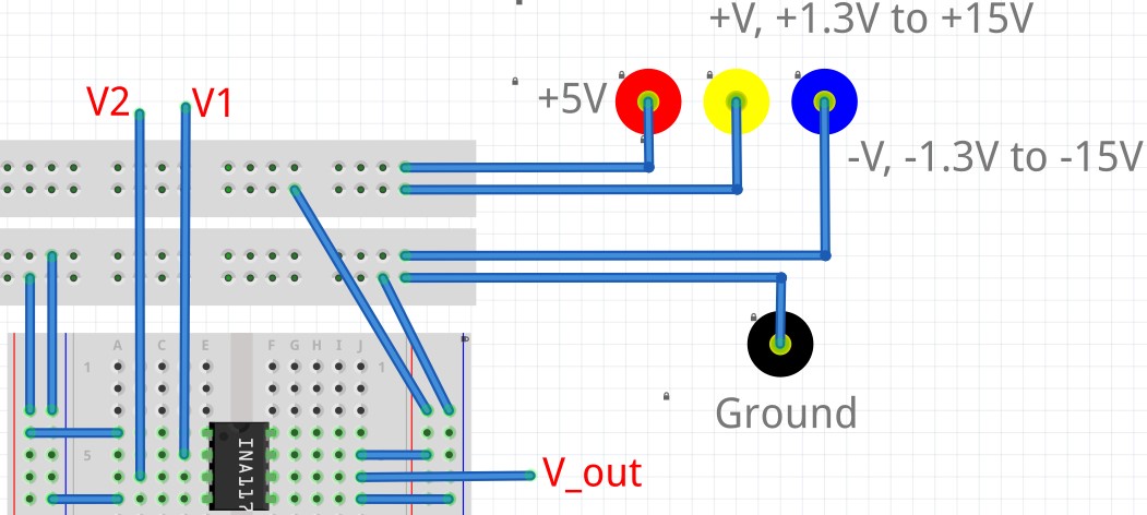
Set up a DMM to measure the variable V+ (yellow) voltage with respect to Ground (black). Pay attention to which of the four top rows correspond to +V and Ground. Turn on the prototyping board.
Adjust the appropriate prototyping board knob so that the +V strip is +15V relative to Ground. Repeat the process above to set -V to be -15V relative to Ground. Do not touch these knobs for the rest of this lab session.
Construct the circuit shown in Figure 11.6.1 on your prototyping board, but leave the smoothing capacitor out of the circuit. The input voltage \(V_\text{in}\) will be provided by your function generator.
Connect the \(\pm 15\)V supplies and Grounds to the INA117P differential amplifier chip as shown in Figure 11.6.2. Note that your instructor should have already inserted the INA117P chip into your prototyping board in the correct orientation.
Turn on the function generator (but leave the OUTPUT disabled). Set the generator to produce a 120-Hz sinusoidal voltage with a peak amplitude of 5-V. Then, enable the OUTPUT.
Adjust the CH1 vertical scale so that the input signal is as large as possible without cutting off any of the signal. Adjust the horizontal timebase such that you can see 3-5 periods of the sinusoidal signal.
Warning: Pay attention to the capacitor polarity in the circuit schematic. If the capacitor is wired in backwards, it may be destroyed (sometimes resulting in a puff of smoke or small flame). Remember that \(V_2 \gt V_1\) always in this circuit.
Enter the CH2 menu and choose AC coupling. This will remove the DC offset and allow you to vertically magnify the display of the AC ripple piece of \(V_\text{out}\text{.}\)
Adjust the CH2 vertical scale to maximize the displayed size of the AC ripple signal and use the oscilloscope’s cursor functionality to measure the peak-to-peak amplitude of the AC ripple.
Perform a curve fit to your \(\left(\Delta V\right)_\text{ripple}\) vs smoothing capacitance data. Assume a function of the form \(\left(\Delta V\right)_\text{ripple}=AC^B\) where \(A\) and \(B\) are fitting parameters and \(C\) is your capacitance variable.