Objective: In your lab notebook, write a few sentences stating your objective in conducting this laboratory exercise. Consider the following questions:
What kind of circuit(s) or components are you exploring?
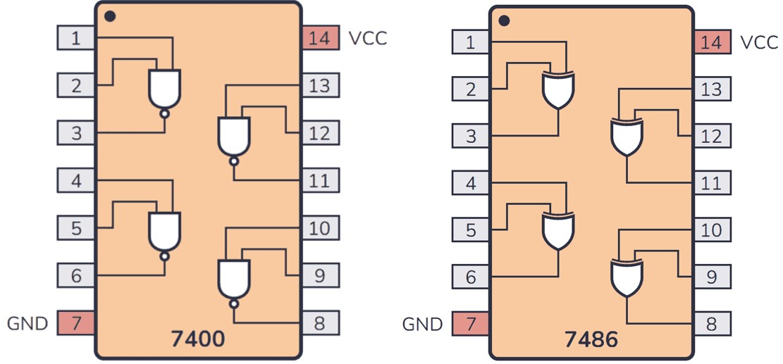
Today we will be looking at an example where we use a digital circuit for computation. While the circuit we examine will be far from our advanced modern computing capabilities, it nonetheless provides insight into some of the foundational building blocks that computing is built upon. We will be using two chips in this circuit, each containing either four NAND gates or four XOR gates. The 74LS00 and 74LS86 pinouts are provided in Figure 11.8.1.
Digital computation uses the binary, or base-2, number system. In the binary number system, we will refer to bits rather than the digits used in a base-10 system. Each digit in a base-10 number can take on any one of 10 values (0-9) which is then multiplied by \(10^n\) where \(n\) is the number of digits to the left of the decimal point. For example, base-10 number 1092 can be understood as \(1\times 10^3 + 0\times 10^2 + 9\times 10^1 + 2\times 10^0\text{.}\) Likewise, each bit in a binary number can take on one of two possible values (0 and 1) with these values multiplying a power of 2. So, the binary number 1011 can be understood as \(1\times 2^3 + 0\times 2^2 + 1\times 2^1 + 1\times 2^0\text{.}\) This means that the binary number 1011 represents 11 in base-10.
The circuit we’ll be examining today is called the digital full-adder.
Figure11.8.2.Circuit schematic for the full-adder circuit. Note: Locations where lines cross in the schematic are only connected if a junction dot appears. There is no connection where wires cross if there is no dot present.
On its own, the full-adder can be used to add two 1-bit numbers represented by \(A_n\) and \(B_n\text{,}\) providing resulting ‘S’um \(S_n\text{.}\) If both \(A_n\) and \(B_n\) are equal to 1, the sum should be equal to 2, but the number 2 is not an allowed value for a bit. So, \(S_n\) will be 1 and we will track the extra that doesn’t fit in \(S_n\) and place the leftover 1 into the ‘C’arry output \(C_{n}\text{.}\) This \(C_n\) result gets carried over into the next higher bit.
Calculations with larger numbers can be completed using multiple full-adders chained together. The circuit in Figure 11.8.3 accepts two 3-bit numbers as inputs and provides an output that is a 4-bit number
Figure11.8.3.Circuit schematic for the full-adder circuit. Note: Locations where lines cross in the schematic are only connected if a junction dot appears. There is no connection where wires cross if there is no dot present.
Build a full-adder using three NAND gates and two XOR gates as shown in Figure 11.8.2. Here are a few tips to help you design the circuit layout on the prototyping board:
Place the 74LS00 and 74LS86 chips across the central vertical gap with a 4-6 row vertical gap between them. The 74LS86 should be above the 74LS00. This may have already been completed by your instructor.
Counting from the left side of the prototyping board, connect the sixth vertical distribution strip (column of vertically-connected holes) to ground and connect the seventh vertical distribution strip to +5 Volts.
Connect each of the third, fourth, and fifth vertical distribution strips to a separate logic switch (labeled \(S_1\) through \(S_8\)). Note: Ensure that the +5 option is selected (rather than the +V option) in the Logic Switch section of the prototyping board. You will use switch \(S_1\) for input \(A_n\text{,}\)\(S_2\) for input \(B_n\text{,}\) and \(S_3\) for input \(C_{n-1}\text{.}\)
Use XOR gates 1 and 2 on the 74LS86 chip. Use NAND gates 1, 2, and 3 on the 74LS00 for the three NAND gates in order from left to right as they appear in Figure 11.8.2
Connect your \(S_n\) and \(C_n\) outputs to pins 1 and 2 in the Logic Indicators section of the prototyping board. Ensure that the +5 and CMOS options are selected with the switches in this section.
Set all circuit inputs to 0 with the logic switches and turn on the board. You should see the first two LOW (green) LEDs light up indicating that outputs \(S_n\) and \(C_n\) are 0 (LOW) when all inputs are low.
Combine the full-adders from multiple groups into a circuit that will compute the base-10 sum \(13+6\text{,}\) providing an answer in binary. Check to make sure that this binary representation converts to the correct base-10 answer. Use Figure 11.8.3 as a guide.
Note: Do NOT disassemble your circuits. I’m asking you to use long wires to connect together circuits from multiple prototyping boards. Your instructor will assist with this process.