So far, we’ve limited our treatment of digital circuits to those with outputs that are fully determined by input values at any given instant. In this section, we’ll study sequential logic, a branch of digial electronics in which circuit outputs depend on input values at that instant in addition to the history of input values. Though the ‘memory’ that we’ll observe in sequential logic circuits is rudimentary compared to that demonstrated by random access memory (RAM) and solid-state drives (SSDs) in computers, the circuits we’ll examine are the fundamental building blocks that make the more advanced applications possible.
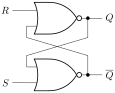
The first sequential logic circuit element that we’ll examine is called a latch. Figure 7.6.1 shows the construction of an SR latch with inputs \(S\text{,}\)\(R\) and outputs \(Q\text{,}\)\(\overline{Q}\text{.}\)
The SR latch is designed such that \(Q=1\) when \(S=1\) and \(R=0\text{;}\) we’ll call this the ‘Set’ state. Likewise, the latch is designed so that \(Q=0\) when \(S=0\) and \(R=1\text{;}\) this is called the ‘Reset’ state. The output labeled \(\overline{Q}\) is in the state opposite to output \(Q\) in both of these cases, the desired result implied by the naming convention used for these outputs. Analysis of the internal NOR gates for these two input states requires that the outputs satisfy
In the Set state, \(S=1\) and \(R=0\text{.}\) Since \(S=1\text{,}\) the bottom NOR gate must produce \(\overline{Q}=0\) regardless of the value of \(Q\text{.}\) Then, since \(R=0\) and \(\overline{Q}=0\text{,}\) the top NOR gate produces \(Q=1\text{.}\) This is a self-consistent solution describing the SR latch behavior.
In the Reset state, \(S=0\) and \(R=1\text{.}\) Since \(R=1\text{,}\) the top NOR gate must produce \(Q=0\) regardless of the value of \(\overline{Q}\text{.}\) Then, since \(S=0\) and \(Q=0\text{,}\) the bottom NOR gate produces \(\overline{Q}=1\text{.}\) This is a self-consistent solution describing the SR latch behavior.
The third input state that we’ll consider is \(S=1\) and \(R=1\text{.}\) Just as for the two cases above, the output state for this case is fully determined by the input state values, resulting in \(Q=0\) and \(\overline{Q}=0\text{.}\) This state will be called the ‘Forbidden’ state and should be avoided in standard operation because the outputs are not inverses of each other as the naming convention indicates they should be.
The final input that we must examine is the case where \(S=0\) and \(R=0\text{.}\) Unlike the cases above, the feedback of output values to the NOR gate inputs must be considered. Combining Eq. (7.6.1) with \(S=R=0\) and Boolean Identity 11 (from List 7.2.1), we find that \(Q=\overline{\overline{Q}}=Q\) and \(\overline{Q} = \overline{Q}\text{.}\) Though these look like identity statements, we must be careful in our interpretation. Logic gates take a finite amount of time to respond and update output values due to changes in input values. If we examine the NOR gate inputs at time \(t=t_0\) and assume a logic gate response time \(\delta t\text{,}\) our analysis would determine output values at \(t_1=t_0 + \delta t\text{.}\) Thus, when \(S(t_0)=0\) and \(R(t_0)=0\text{,}\) we find \(Q(t_1)=\overline{R(t_0) + \overline{Q(t_0)}} = Q(t_0)\) and \(\overline{Q(t_1)} = \overline{S(t_0) + Q(t_0)}=\overline{Q(t_0)}\text{.}\) We’ll call this the ‘Hold’ state since both \(Q\) and \(\overline{Q}\) remain unchanged with whatever values they held before entering the Hold state.