Having established the behavior of flip-flops, we move on to applications that make use of these circuit elements. In particular, we will examine shift registers and the counters that are based on them.
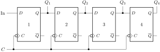
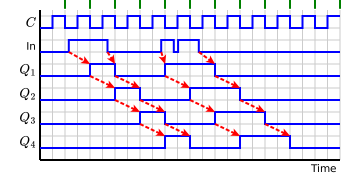
In this circuit, the input signal (In) is assumed to be controlled by some external source (another circuit or a person) and can change between high and low at any time. Output \(Q_0\) reproduces an approximation to this input signal, though only allows changes between low and high on the negative edge of the clock signal CLK. In a sense, the ‘resolution’ with which the flip-flop reproduces the input signal is limited by the CLK frequency which is why the pulse lengths in \(Q_0\) are not identical to those in the input signal and is why the circled input signal transitions do not appear in \(Q_0\text{.}\) Outputs \(Q_1\text{,}\)\(Q_2\text{,}\) and \(Q_3\) are all identical to \(Q_0\) except that each output is time delayed by \(\Delta t=1/f_\text{CLK}\) from the output before it. Figure 7.8.2 shows this behavior where circuit outputs at some instant are not dependent on the input at that instant. Instead, \(Q_1\text{,}\)\(Q_2\text{,}\) and \(Q_3\) depend on the state of \(Q_0\) progressively further in the past and \(Q_0\) is a sampled version of the input signal. Memory in this context is represented by circuit output behavior that is based on past rather than present input signal behavior.
Figure7.8.2.This shift register timing diagram reflects the behavior of the shift register circuit in Figure 7.8.1. The output \(Q_0\) represents the sampling of the input signal based on the negative edge triggering of flip-flop 1. Outputs \(Q_1\text{,}\)\(Q_2\text{,}\) and \(Q_3\) are identical to \(Q_0\) except they are time delayed by one clock period relative to the previous output signal.
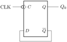
We can use the memory functionality demonstrated by flip-flop circuits above to produce a circuit that counts. Let’s first start with the flip-flop configuration that is called a mod-2 counter. This circuit, shown in Figure 7.8.3, takes a square-wave clock input and produces a square-wave output with half of the clock’s frequency.
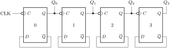
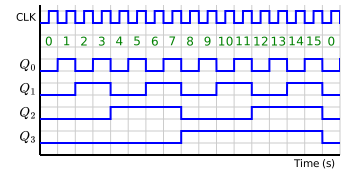
The circuit shown in Figure 7.8.4 uses four mod-2 counters in a cascading configuration. The output of one mod-2 counter serves as the input to the next mod-2 counter in the chain, resulting in square-wave outputs that have frequencies that get progressively smaller by a factor of two for each subsequent flip-flop. This circuit is called an asynchronous 4-bit counter. It counts from 0 to 15 in binary before resetting to 0, with \(Q_i\) representing the value of the \(i\)-th bit of a 4-bit number as a function of time.
The term asynchronous is used because the four flip-flops in the circuit are not triggered at the same time. Instead, each flip-flop is triggered by changes in the output state of the flip-flop appearing to its left. Because a flip-flop takes a finite time to change its output upon triggering, this leads to a ripple effect in which a small delay in flip-flop triggering propagates left to right through the counter circuit.
Figure7.8.5.Timing diagram for the asynchronous 4-bit counter.
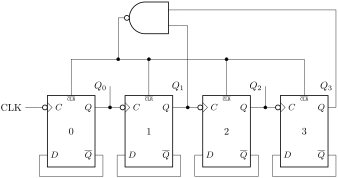
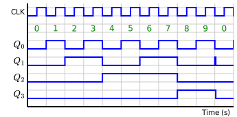
The Preset and Clear flip-flop inputs can be used to modify the asynchronous 4-bit counter circuit in Figure 7.8.4 to truncate the count and cause the counter to reset before it reaches 15. For example, an asynchronous decade counter will count from 0-9 before resetting back to 0. In order to truncate the count, the circuit must reset to the 4-bit binary number 0000 instead of proceeding to 1010 (the binary equivalent to the digit 10). So, the circuit must send a clear signal to all four flip-flops immediately upon the outputs reaching \(Q_3=1\text{,}\)\(Q_2=0\text{,}\)\(Q_1=1\text{,}\) and \(Q_0=0\text{.}\) This condition can be simplified as this output is the first time at which both \(Q_3=1\) and \(Q_1=1\) simultaneously. Since the CLR inputs are active low, a single NAND gate provides this truncation when the gate has inputs \(Q_1\text{,}\)\(Q_3\) and an output that connects to all four flip-flop CLR inputs. Figure 7.8.6 shows the asynchronous decade counter circuit while Figure 7.8.7 shows the counting functionality.